
| Part1 - Wanna see my parts? | |
| In Part1 of this tutorial we will go through the entire process of stuffing, soldering and testing the Zero Point SDX PCB. This is a complicated build and you should expect to spend an hour or two getting through all the steps. Take your time, relax, and most of all: enjoy yourself! | |
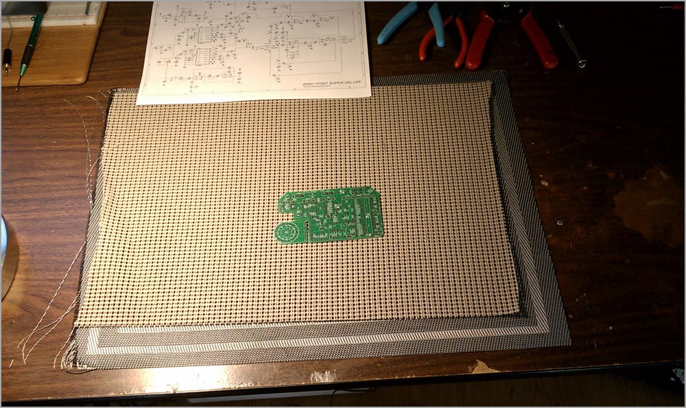 |
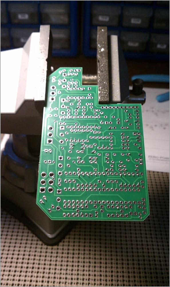
I always start with a clean workspace. In a complicated and lengthy build like this one it is pretty necessary. Here I have my Zero Point Schematic and PCB ready to go. |
My workspace is set up so that all my components and hardware are stored neatly in these boxes. Everything is labeled and easy to read. This makes building a breeze, since I can reach just about everything from a sitting position. |
 |
 |
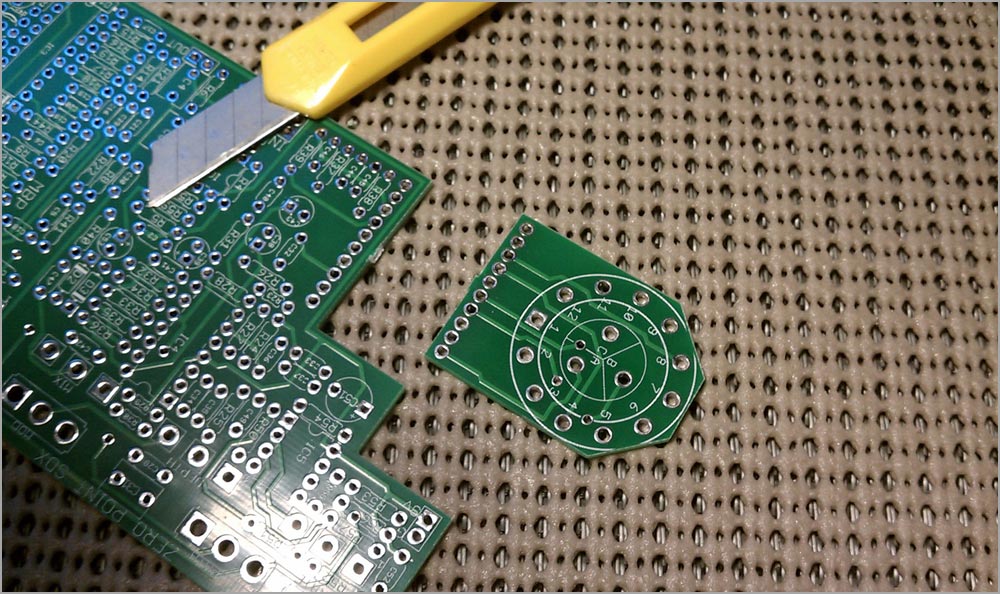
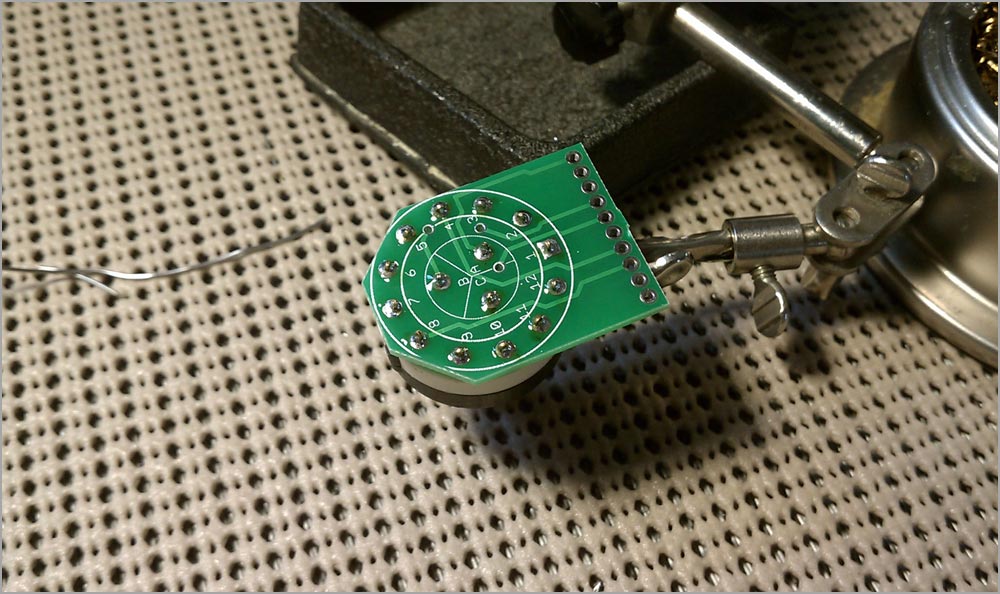
Before we begin populating the PCB, we need to snap off the breakout board for the rotary switch. Use a wire cutter to cut the bridge between the two boards. Careful! That little board might go flying when you cut. Mine went about 5 feet. |
An Xacto knife can trim up the edges of the two PCBs to make it cleaner looking. The PCB material is pretty easy to shave off this way. |
 |
 |
For this build, I’m going to load all the resistors first. Usually, I load ALL components before soldering. But, since this is a demonstration we’ll do it in pieces. Here’s R1 loaded with the leads bent inward to hold it in place. |
Cut the leads close to the outer edge of the solder pad. It’s important to cut them correctly. Too short and the component may fall out. Too long and you have excess. |
 |
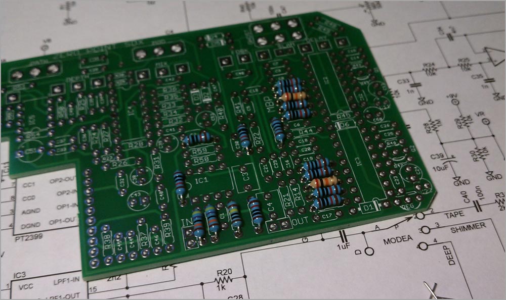 |
Keep working on stuffing those resistors. I generally go pretty linear from R1 to Rz. |
Here are most of the resistors loaded. I left off R45 per the most recent update to the build document. I’ve also left off R21 and R22 which I plan to socket. These are the two resistors that will determine the level of the multiple repeats in “Ghost” mode, and I want to experiment with them later on. The build doc also suggests using a 470k or higher for R48 to limit the max delay. I chose 750k…well, just because. Lastly, I’ve put a few of the diodes in. |
 |
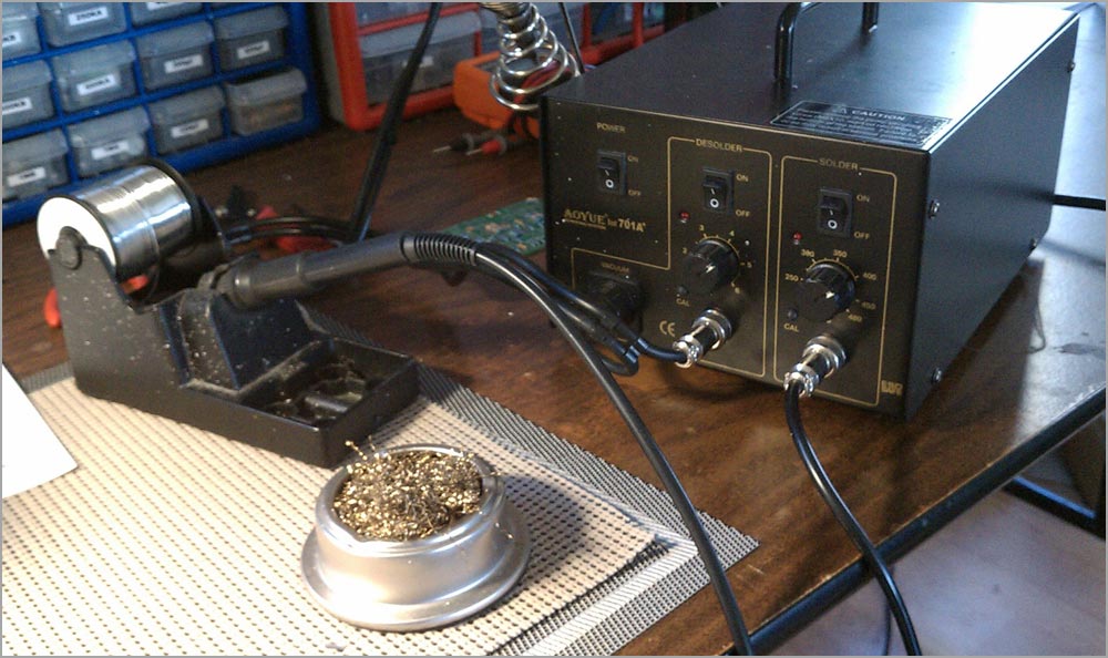 |
Now we can do some soldering! Here’s my current solder station. It’s an AOYUE 701A which has both soldering and desoldering capabilities. I cannot live without the desolder pump…it’s essential to building lots and lots of circuits. |
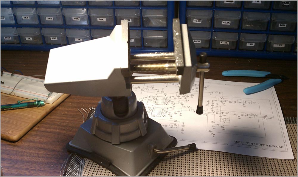
I also use a vise to hold my PCBs when I solder. I bought this one at Lowe’s, I think. |
 |
 |
The vise does not open far enough to accommodate the entire width of the PCB. That’s okay. I just clamp it at the cutout. |
Tin that solder tip before you start! Get a small blob on it and let it heat for a few seconds. Here’s my solder tip, tinned and ready to go. |
 |
 |
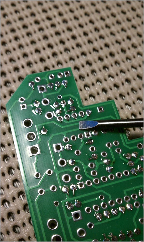
To solder, place you tip so that it contacts both the pad and component lead. Wait about 3 seconds for them to heat up. At this point, solder should start to flow over the pad and lead smoothly. It’s important to not use either too much or too little. These solder joints are pretty good…maybe just a tad on the low side solder-wise. I actually did that on purpose (no, really!) because I’m going to top solder these resistors later. |
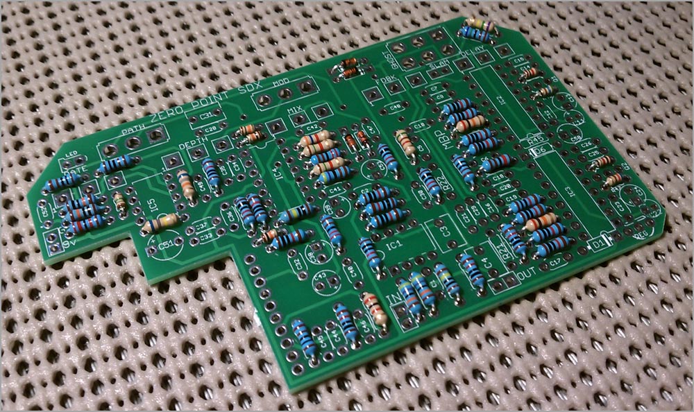
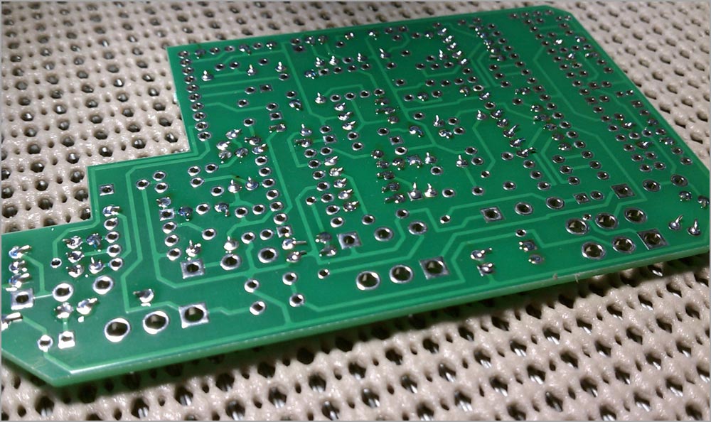
Here are the resistors soldered up. It takes a while, but it is important to be patient and thorough. At the same time, don’t be too meticulous. You can always go back and touch up your solder joints as the build moves along. I’ll inspect and reflow some of these joints a few times during the build. |
 |
 |
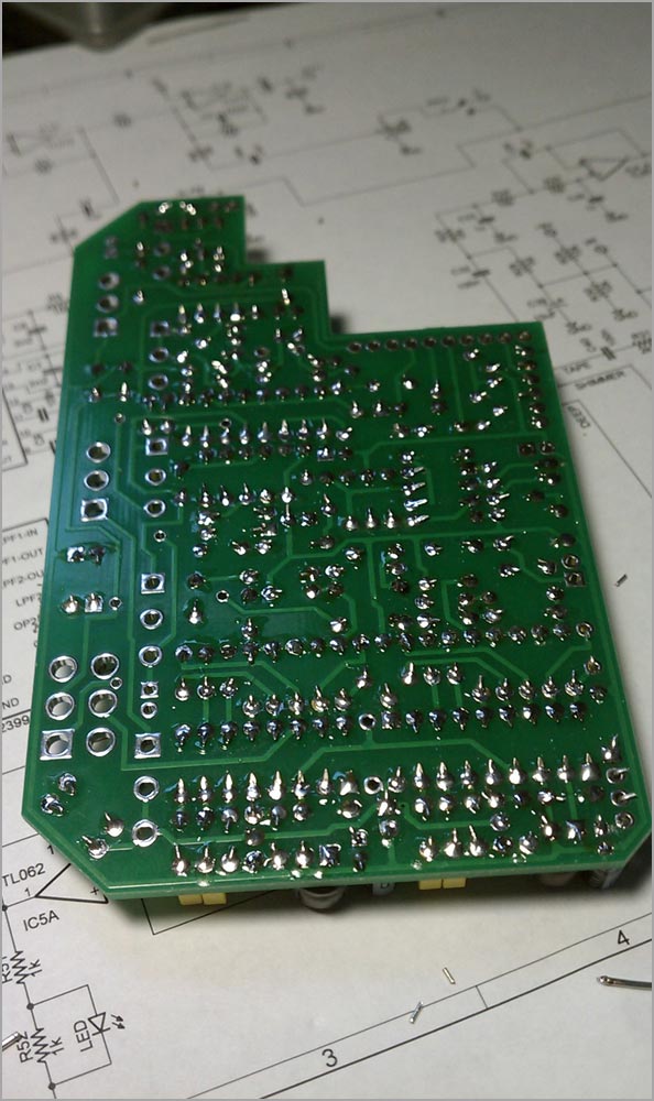
Here’s the top of the PCB with the resistors. As you can see, solder has flowed through the pads. Since I have plenty of room to work, I’m going to do some quick touch up on the top and reflow joints adding solder where needed. You don’t have to top solder. But, it does give it a more professional look AND makes the components more secure. |
The top soldering is done. Wow! Looks freakin good. If you do this, you are already light years ahead of most ‘booteek’ pedal builders. |
 |
 |
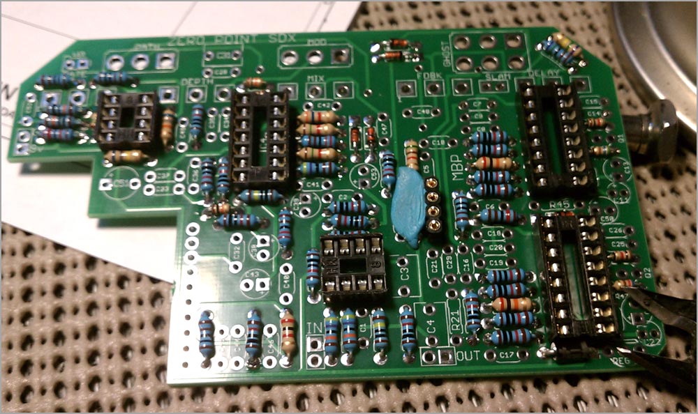
Now that the resistors are done, let’s load some sockets. There’s no reason not to socket ICs. It makes it easy to swap them out if they go south, prevents heat damage from soldering and they are cheap. IOW, do it, brah! I’m using cheap leaf pin sockets I bought from Tayda. I generally use a small flathead edge to bend the pins inward to hold it in. |
Here are the IC sockets loaded and soldered. See all that blue smurf goo? That’s BluTac. It’s perfect for temporarily holding straight pin sockets in place when soldering. I use the Tac stuff for all kinds of things in building. |
 |
 |
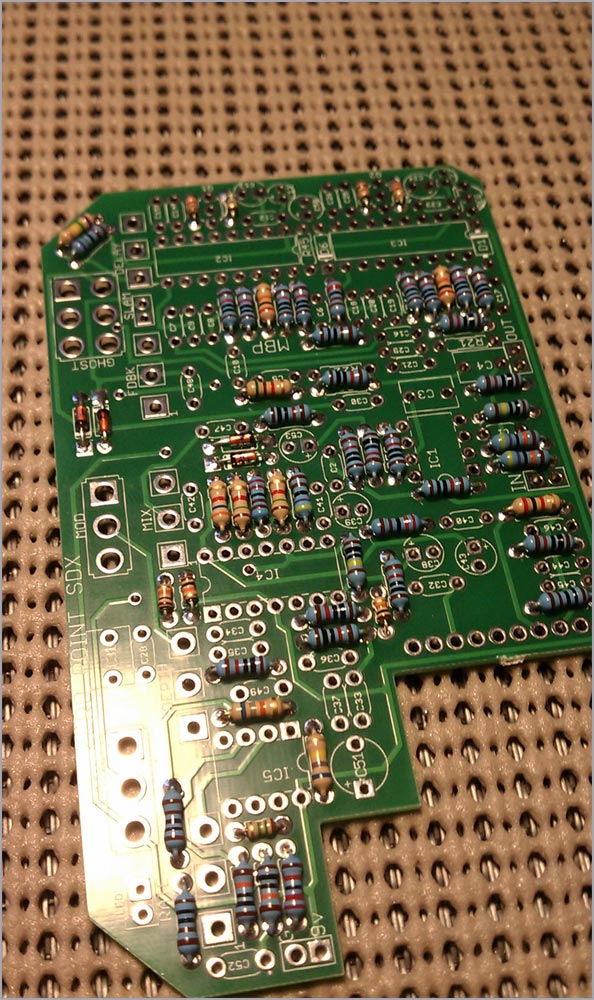
Let’s keep moving and load all the capacitors. I’m using a mix of flavors here: AVX box caps (no, you cannot get these any more), electrolytic, ceramic and a couple of tantalums. The build doc suggests 10uF tants for the 5vDC filtering for the two PT2399s, but I am out of them. So, I used regular electrolytic. I also used a couple of 1uF tantalum in the ‘Modes” section. No particular reason…I just happen to have a lot of 1uFs to use up. |
Lots of tasty solder joints here. See how they shine? If you look really close, you’ll see that I missed a few. Oops! That’s okay: I catch all of them later on as I’m building. |
 |
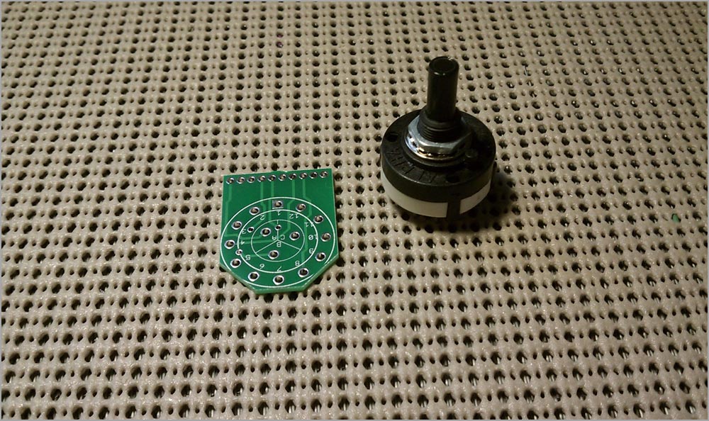 |
Let’s tackle the breakout board. Here’s my 3P4T rotary switch (pin mounted). The switch goes under the PCB. Notice that the PCB has labels for A, B and C which match those on the rotary switch. Line those up and plunk it down (actually it will still work even if you don’t line up A to A…but pretend you don’t know that). |
I broke out my Radio Shack “Helping Hands” to hold the rotary switch while I solder the pins and pads together. This is a handy little tool which I use for every build, like the big vise. |
 |
 |
I’m going to use some standoff pins to join the main board and breakout board. I happen to have the correct ones, which are .1” spacing. This is a lot easier than soldering wires for each and every connection. |
Here are the pins soldered to the main PCB. This is actually a mistake, but I don’t realize it until later. It’s better to NOT solder these to the main PCB now. With the pins soldered to the main board, it gets pretty hard to line the rotary up evenly. I’ll fix this later on in the tutorial. We’ve made a lot of progress so far! Take a break, have some coffee, a smoke, or check your email. Also, don’t smoke. But if you do, then do that now. Ahhhh. Why are you still here? Shouldn’t you be taking a break? Oh, you want to keep going? Alright then, let’s get on to the potentiometers.. |
 |
 |
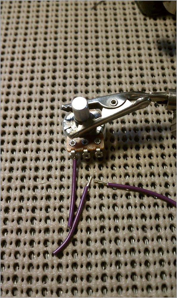
I’m running pretty low on PCB pin mounted pots, so I will be using a mixture. My only 1MC is pin mounted, and the others are solder lugs. Not a big deal. I’ll show you how to use both without anyone ever knowing the difference. I’m also using these clear dust covers I bought from Smallbear. They prevent the pot casings from contacting (and shorting) any solder joints on the PCB. |
This is how I typically wire pots. I use the Helping Hands to hold the shaft then thread the wire though the lug. You can do all three wires in one pass. |
 |
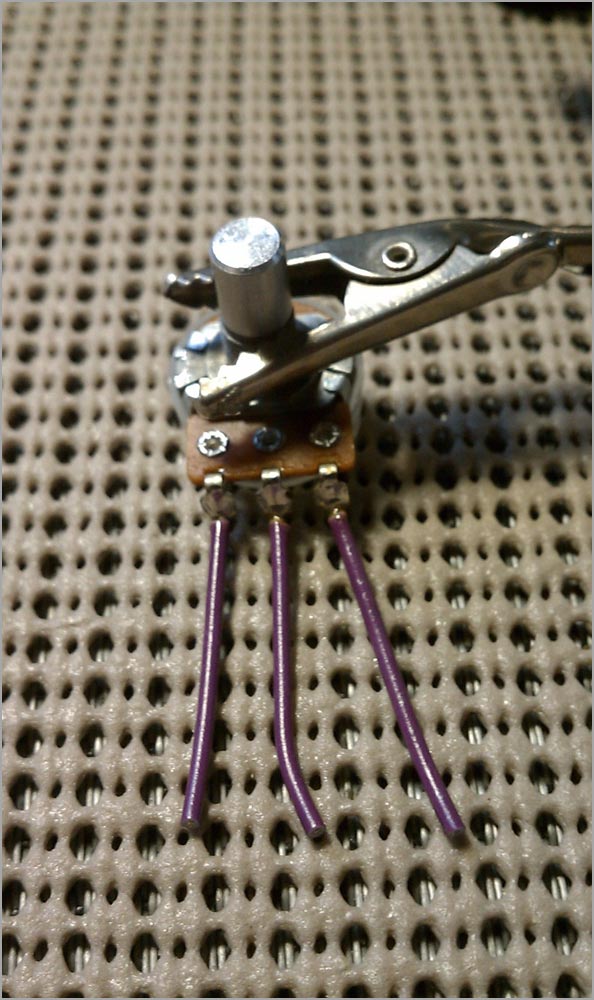 |
Here are the three wires soldered to the pot. Notice how I keep the exposed wire pretty short? |
I’ve trimmed the insulation very close on the wires. This will allow me to bend them up and mount them as if it were a pin mounted pot. |
 |
 |
Here’s a comparison between the pin mounted and wired pot. See how they line up perfectly? |
All the pots have been soldered to the board. Since I bent the wires down at a 90° angle, I've added a little extra solder over each lug to strengthen the contact points. |
 |
 |
Next up we have three switches: two SPDTs and a DPDT (all On/On). |
Time for a bit more smurf goo! Seriously, BluTac is magic. |
 |
 |
All the switches are now soldered to the main PCB. |
At this point, I realize the mistake I made earlier with the rotary switch. The problem is that the shaft of the rotary is longer than that of the switches and pots. I can’t seem to find a good way to brace the two PCBs so that the pins sit flush on the main PCB. So, I de-soldered the pin headers from the main board and re-solder them to the breakout board. |
 |
 |
This allows me to flip both PCBs over and solder from the bottom while keeping the two PCBs aligned properly. |
The rotary switch and breakout PCB are now lined up correctly and soldered in place. |
 |
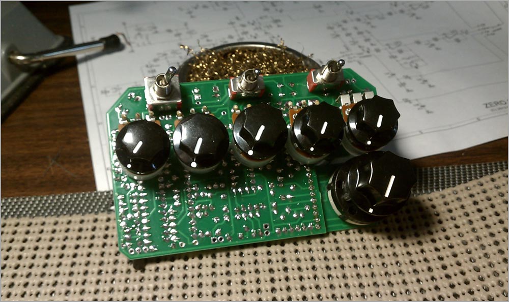 |
Man, we are getting close! Here I have temporarily mounted some knobs on the pots and switch. This is really useful when testing out your build since it gives you a visual indicator on what the controls are doing. |
Yup, the DC jack is going to fit just fine in the pocket between the two PCBs and over the Rate pot. Whew! |
 |
 |
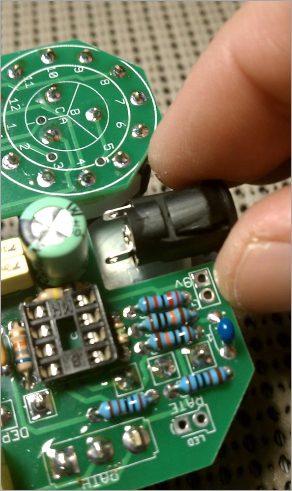
Time to start wiring this bad boy up! At this stage, I have wired the 9v, one ground, input, output and the pads for the “Slam” switch. I’m not going to actually wire switches out of the box. Rather, I will just connect them up as need to my testing rig. This makes the whole rig a lot easier to handle and flip around (which I may have to do if the build is not working properly). I’ll wire up the other ground wires later when I’m ready to box…no need at this point. |
A bottom shot….just because. (Actually, this also shows the LED. I've made a guess as to the proper height. I can always fix the position later, if needed.) |
 |
 |
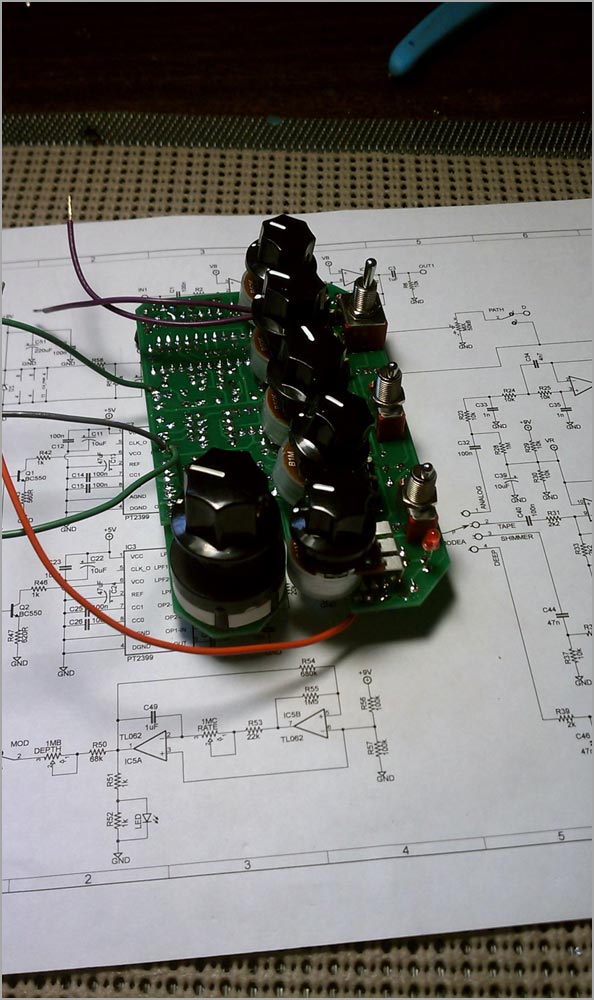
Here’s the testing rig I use for ALL my builds. It is really simple: a box with input, output, DC and LED to simulate how it will be in the final pedal. The breadboard on the left has some stuff in case I need to regulate voltage (not needed in this build). The other breadboard has 9v and ground on the top and bottom rows, and input and output connections. I cannot emphasize this enough: MAKE A TESTING RIG! Never, ever box a new build before testing it out. You are just setting yourself up for a lot of hassle if your build is not working. IOW, ROCK IT BEFORE YOU BOX IT, YO. |
Before loading the ICs on the PCB we should test voltages. I've connected power and ground to the test rig. Using my DMM I check the corresponding pins on each IC socket to verify that I am getting the correct voltage and grounds. The PT2399s get 5vDC and all the other get 9v. Looks like we are good to go! |
 |
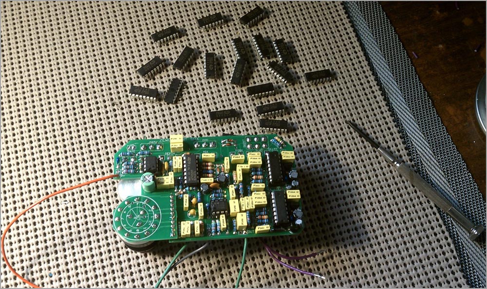 |
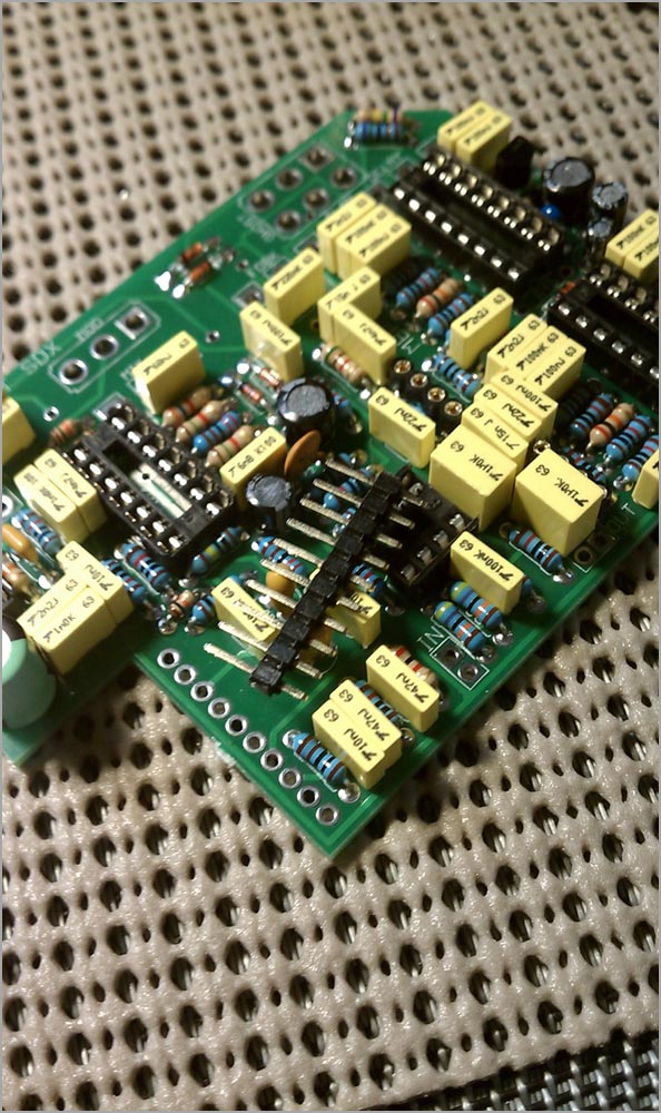
ICs are now loaded onto the PCB. I’ve also dumped a mess of extra PT2399s on the bench. I have a bunch from different sources: Tayda, eBay, Smallbear, etc. Given the prevalence of fake ICs AND the seeming inconsistency from chip to chip, I might end up trying a few of these in the build to find the ones with the lowest noise. It’s a good idea to have either a few on hand, or a supply from a trusted source. |
| Go to Part 2! | |
 |
 |
 |
 |
 |
 |
 |